YuSynth Random gates
Introduction
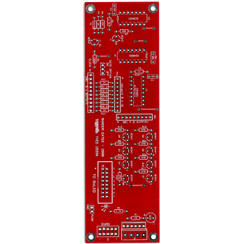
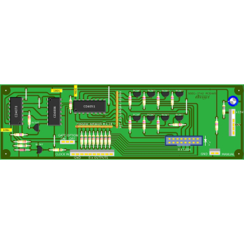
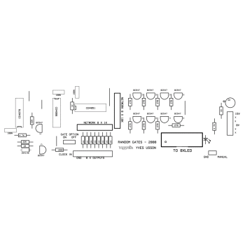
A bare double sided PCB (no need for the wire jumper links shown on the PCB layout) for the Yusynth Random Gates synth module. These PCBs are manufactured by Soundtronics with a percentage of the sale going to the creator of the YuSynth - Yves Usson. These are early days for the YuSynth Modular Synth at Soundtronics, our plan is to stock PCBs for all of the projects as well as components, kits and front panels. This is going to take time but will eventually be as comprehensive as our MFOS range.
No components are included with the PCB but check out our Synth Components section where you should find what you need. We do suggest visiting the YuSynth Random Gates project page for detailed information including Yves panel layouts but a summary is shown below.
Description
When Yves designed this module, he had in mind to control a Moog 960 sequencer in a random fashion, but many other applications may be imagined. On the 960 sequencer, a single step can be selected directly by it's IN jack, that is, instead of having the step sequenced in the logical sequence order you may call every step in an arbitrary order provided that you address directly each step with the IN jacks. The Octal Random Gate provides eight GATE OUT signals that are randomly sequenced, that is, one out of eight output is active and this randomly changes at every clock pluse. Therefore, at each clock pulse sent to the GATE IN a randomly selected output is set to the ON state while all the other outputs are set to the OFF state.
A toggle switch makes it possible to choose the gating mode between two modes: in the first mode the ON status of the selected output lasts until the next clock pulse; in the second mode, the ON status is gated by the clock pulse, that is it lasts as long as the clock pulse is at the ON status and returns to OFF as soon as the clock signal returns to OFF (see diagram below : output X selected during one clock cycle, output Y selected during two consecutive clock cycles; left GATE MODE OFF, right GATE MODE ON).
IMPORTANT NOTE :
Yves has modified the schematic and PCB of this module because there has reports of problems with the previous PCB when using HEF4006 or MC14006 instead of the CD4006 for which the circuit was designed. As the matter of fact, the HEF4006 and the MC14006 both require very steep clock edges to work properly while the CD4006 can handle slopier edges. Yves modified the circuit to convert one of the unused XOR gates of the 4070 into a pulse straightener.
The PCB can accept a choice of three types of power connector, it can be either a Synthesizers.com 6 pins MTA connector, a MOTM 4 pins MTA96 connector or a 10-pin Eurorack connector.
Circuit
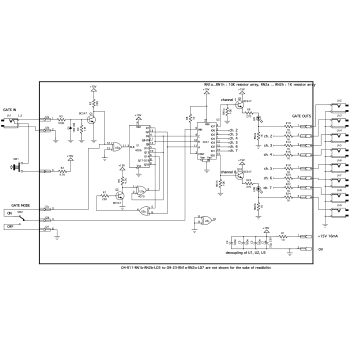
Click on the schematic thumbnail above for the circuit diagram.
Basically, the circuit contains three main parts : the clock input built with Q1, the pseudo random sequence generator built with Q2, U1 and U3; and the addressing and output stages built with U2 and Q3 to Q10.
The core of the module is the pseudo-random sequence generator, it is in fact a classical circuit (Elektor) uses to generate digital noise. The CD4006 is an eighteen stage shift register whose some of its outputs are fedback to its input through XOR gates (CD4070). Q2 inverses one of the output before applying to the XOR gate input in order to avoid an all zero status that would block the generator. The random generator is clocked by an external signal which is buffered by Q1, then a XOR gate of U3d is used to straighten the edges of the clock pulses : this was necessary to make this circuit work with some brands of the 4006 (HEF4006,MC14006) which required more stringent pulse conditions. Three outputs of the CD4006 are connected to the binary addressing pins (A,B,C) of the CD4051 (8 voice analogue multiplexer). The common pin of the CD4051 is connected to the positive rail through a 1K resistor, and all the outputs are connected to an output buffer stage. The GATE MODE switch controls the INHIBIT pin of the CD4051, in the OFF mode the INHIBIT pin is connected to the ground and the active output of the CD4051 remains active. In the ON mode the clock signal is routed to the INHIBIT pin and gates the active output.
NOTE : after powering up, the module needs at least ten clock cycles before it gets into the expected behaviour.
Wiring
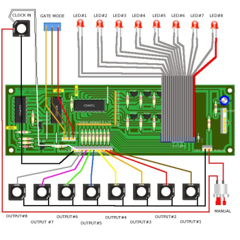
The wiring schematic image in the above thumbnails show the panel wiring to the pots and sockets etc.
Setting and Trimming
No trimming is required
Parts List
The parts list below is direct from the YuSynth website. Please see this revised BOM that better reflects the YuSuynth PCB and schhematic.
The parts list excludes knobs although we have standardised on the Cliff KM20B but it does include 1/4" jack sockets. All parts are available individually (use the part number in the search box above) or as a components kit that excludes sockets and knobs.
Reference | Value | Part No. | Qty |
U1 | CD4006 (also working with HEF4006 or MC14006) | 7212-507 | 1 |
U2 | CD4051 | 7212-513 | 1 |
U3 | CD4070 | 7212-516 | 1 |
Q1,Q2,Q3,Q4,Q5,Q6,Q7,Q8,Q9,Q10 | BC547 | 7212-401 | 10 |
D1 | 1N4148 | 7212-480 | 1 |
R1 | 10 ohm | 7163-007 | 1 |
R17,R18,R19,R27,R28,R29,R37,R38,R39 | 270 ohm | 7163-037 | 8 |
R8,R10,R12,R14,R16,R18,R20,R22,R24 | 1K | 7163-051 | 9 |
R9,R11,R13,R15,R17,R19,R21,R23 | 4.7k | 7163-067 | 8 |
R5,R7 | 22k | 7163-083 | 2 |
R3 | 100k | 7163-099 | 1 |
R4 | 1M | 7163-122 | 1 |
RN2 | Resistor network 8x1K one common leg | 7212-830 | 1 |
RN1 | Resistor network 8x10K one common leg | 7212-831 | 1 |
C2,C3,C4 | 100nF | 7212-749 | 3 |
C1 | 10µF or 22µF/35V electro. | 7213-119 | 1 |
Jk1,Jk2,Jk3,Jk4,Jk5,Jk6,Jk7,Jk8,Jk9 | 6,5 mm jack socket | 7212-209 | 9 |
J1 | HE10 male socket 2x8 pins | 7212-313 | 1 |
HE10 female connector 2x8 pins | 7212-310 | 1 | |
16 lead flat ribon 20cm | 7210-120 | 1 | |
SW1 | Push button | 7212-253 | 1 |
SW2 | bipolar switch SPDT | 7212-250 | 1 |